

TDA7294 - Datasheet Catalog
TDA7294 - Datasheet Catalog
TDA7294 - Datasheet Catalog

Create successful ePaper yourself
Turn your PDF publications into a flip-book with our unique Google optimized e-Paper software.
®<br />
<strong>TDA7294</strong><br />
100V - 100W DMOS AUDIO AMPLIFIER WITH MUTE/ST-BY<br />
VERY HIGH OPERATING VOLTAGE RANGE<br />
(±40V)<br />
DMOS POWER STAGE<br />
HIGH OUTPUT POWER (UP TO 100W MU-<br />
SIC POWER)<br />
MUTING/STAND-BY FUNCTIONS<br />
NO SWITCH ON/OFF NOISE<br />
NO BOUCHEROT CELLS<br />
VERY LOW DISTORTION<br />
VERY LOW NOISE<br />
SHORT CIRCUIT PROTECTION<br />
THERMAL SHUTDOWN<br />
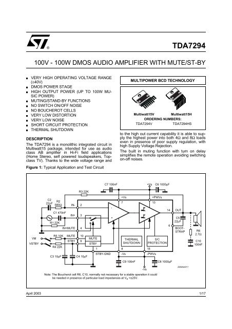
DESCRIPTION<br />
The <strong>TDA7294</strong> is a monolithic integrated circuit in<br />
Multiwatt15 package, intended for use as audio<br />
class AB amplifier in Hi-Fi field applications<br />
(Home Stereo, self powered loudspeakers, Topclass<br />
TV). Thanks to the wide voltage range and<br />
MULTIPOWER BCD TECHNOLOGY<br />
Multiwatt15V Multiwatt15H<br />
ORDERING NUMBERS:<br />
<strong>TDA7294</strong>V<br />
<strong>TDA7294</strong>HS<br />
to the high out current capability it is able to supply<br />
the highest power into both 4Ω and 8Ω loads<br />
even in presence of poor supply regulation, with<br />
high Supply Voltage Rejection.<br />
The built in muting function with turn on delay<br />
simplifies the remote operation avoiding switching<br />
on-off noises.<br />
Figure 1: Typical Application and Test Circuit<br />
C7 100nF +Vs C6 1000µF<br />
R3 22K<br />
VM<br />
VSTBY<br />
C2<br />
22µF<br />
R2<br />
680Ω<br />
C1 470nF<br />
R1 22K<br />
R5 10K<br />
R4 22K<br />
IN- 2<br />
IN+<br />
IN+MUTE<br />
MUTE<br />
STBY<br />
3<br />
4<br />
10<br />
9<br />
MUTE<br />
STBY<br />
1<br />
-<br />
+<br />
+Vs<br />
7 13<br />
8<br />
THERMAL<br />
SHUTDOWN<br />
S/C<br />
PROTECTION<br />
15<br />
+PWVs<br />
14<br />
6<br />
OUT<br />
C5<br />
22µF<br />
BOOT-<br />
STRAP<br />
R6<br />
2.7Ω<br />
C10<br />
100nF<br />
C3 10µF C4 10µF<br />
STBY-GND<br />
-Vs<br />
-PWVs<br />
C9 100nF C8 1000µF<br />
-Vs<br />
D93AU011<br />
Note: The Boucherot cell R6, C10, normally not necessary for a stable operation it could<br />
be needed in presence of particular load impedances at V S
<strong>TDA7294</strong><br />
PIN CONNECTION (Top view)<br />
TAB connected to -V S<br />
BLOCK DIAGRAM<br />
ABSOLUTE MAXIMUM RATINGS<br />
Symbol Parameter Value Unit<br />
V S Supply Voltage (No Signal) ±50 V<br />
I O Output Peak Current 10 A<br />
P tot Power Dissipation T case = 70°C 50 W<br />
T op Operating Ambient Temperature Range 0 to 70 °C<br />
T stg , T j Storage and Junction Temperature 150 °C<br />
2/17
<strong>TDA7294</strong><br />
THERMAL DATA<br />
Symbol Description Value Unit<br />
R th j-case Thermal Resistance Junction-case Max 1.5 °C/W<br />
ELECTRICAL CHARACTERISTICS (Refer to the Test Circuit VS = ±35V, RL = 8Ω, GV = 30dB;<br />
Rg = 50 Ω; Tamb = 25°C, f = 1 kHz; unless otherwise specified.<br />
Symbol Parameter Test Condition Min. Typ. Max. Unit<br />
V S Supply Range ±10 ±40 V<br />
I q Quiescent Current 20 30 65 mA<br />
I b Input Bias Current 500 nA<br />
V OS Input Offset Voltage +10 mV<br />
I OS Input Offset Current +100 nA<br />
P O RMS Continuous Output Power d = 0.5%:<br />
V S = ± 35V, R L = 8Ω<br />
V S = ± 31V, R L = 6Ω<br />
V S = ± 27V, R L = 4Ω<br />
Music Power (RMS)<br />
IEC268.3 RULES - ∆t = 1s (*)<br />
d = 10%<br />
R L = 8Ω ; V S = ±38V<br />
R L = 6Ω ; V S = ±33V<br />
R L = 4Ω ; V S = ±29V (***)<br />
d Total Harmonic Distortion (**) P O = 5W; f = 1kHz<br />
P O = 0.1 to 50W; f = 20Hz to 20kHz<br />
V S = ±27V, R L = 4Ω:<br />
P O = 5W; f = 1kHz<br />
P O = 0.1 to 50W; f = 20Hz to 20kHz<br />
0.01<br />
%<br />
0.1 %<br />
SR Slew Rate 7 10 V/µs<br />
G V Open Loop Voltage Gain 80 dB<br />
G V Closed Loop Voltage Gain 24 30 40 dB<br />
e N Total Input Noise A = curve<br />
f = 20Hz to 20kHz<br />
60<br />
60<br />
60<br />
70<br />
70<br />
70<br />
100<br />
100<br />
100<br />
0.005<br />
0.1<br />
1<br />
2 5<br />
f L, f H Frequency Response (-3dB) P O = 1W 20Hz to 20kHz<br />
R i Input Resistance 100 kΩ<br />
SVR Supply Voltage Rejection f = 100Hz; V ripple = 0.5Vrms 60 75 dB<br />
T S Thermal Shutdown 145 °C<br />
STAND-BY FUNCTION (Ref: -V S or GND)<br />
V ST on Stand-by on Threshold 1.5 V<br />
V ST off Stand-by off Threshold 3.5 V<br />
ATT st-by Stand-by Attenuation 70 90 dB<br />
I q st-by Quiescent Current @ Stand-by 1 3 mA<br />
MUTE FUNCTION (Ref: -V S or GND)<br />
V Mon Mute on Threshold 1.5 V<br />
V Moff Mute off Threshold 3.5 V<br />
ATT mute Mute AttenuatIon 60 80 dB<br />
Note (*):<br />
MUSIC POWER CONCEPT<br />
MUSIC POWER is the maximal power which the amplifier is capable of producing across the rated load resistance (regardless of non linearity)<br />
1 sec after the application of a sinusoidal input signal of frequency 1KHz.<br />
Note (**): Tested with optimized Application Board (see fig. 2)<br />
Note (***): Limited by the max. allowable current.<br />
W<br />
W<br />
W<br />
W<br />
W<br />
W<br />
%<br />
%<br />
µV<br />
µV<br />
3/17
<strong>TDA7294</strong><br />
Figure 2: P.C.B. and components layout of the circuit of figure 1. (1:1 scale)<br />
Note:<br />
The Stand-by and Mute functions can be referred either to GND or -VS.<br />
On the P.C.B. is possible to set both the configuration through the jumper J1.<br />
4/17
<strong>TDA7294</strong><br />
APPLICATION SUGGESTIONS (see Test and Application Circuits of the Fig. 1)<br />
The recommended values of the external components are those shown on the application circuit of Figure<br />
1. Different values can be used; the following table can help the designer.<br />
COMPONENTS SUGGESTED VALUE PURPOSE<br />
LARGER THAN<br />
SUGGESTED<br />
SMALLER THAN<br />
SUGGESTED<br />
R1 (*) 22k INPUT RESISTANCE INCREASE INPUT<br />
IMPRDANCE<br />
DECREASE INPUT<br />
IMPEDANCE<br />
R2 680Ω CLOSED LOOP GAIN DECREASE OF GAIN INCREASE OF GAIN<br />
SET TO 30dB (**)<br />
R3 (*) 22k INCREASE OF GAIN DECREASE OF GAIN<br />
R4 22k ST-BY TIME<br />
CONSTANT<br />
R5 10k MUTE TIME<br />
CONSTANT<br />
C1 0.47µF INPUT DC<br />
DECOUPLING<br />
C2 22µF FEEDBACK DC<br />
DECOUPLING<br />
C3 10µF MUTE TIME<br />
CONSTANT<br />
C4 10µF ST-BY TIME<br />
CONSTANT<br />
LARGER ST-BY<br />
ON/OFF TIME<br />
LARGER MUTE<br />
ON/OFF TIME<br />
LARGER MUTE<br />
ON/OFF TIME<br />
LARGER ST-BY<br />
ON/OFF TIME<br />
SMALLER ST-BY<br />
ON/OFF TIME;<br />
POP NOISE<br />
SMALLER MUTE<br />
ON/OFF TIME<br />
HIGHER LOW<br />
FREQUENCY<br />
CUTOFF<br />
HIGHER LOW<br />
FREQUENCY<br />
CUTOFF<br />
SMALLER MUTE<br />
ON/OFF TIME<br />
SMALLER ST-BY<br />
ON/OFF TIME;<br />
POP NOISE<br />
C5 22µF BOOTSTRAPPING SIGNAL<br />
DEGRADATION AT<br />
LOW FREQUENCY<br />
C6, C8 1000µF SUPPLY VOLTAGE<br />
BYPASS<br />
C7, C9 0.1µF SUPPLY VOLTAGE<br />
BYPASS<br />
DANGER OF<br />
OSCILLATION<br />
DANGER OF<br />
OSCILLATION<br />
(*) R1 = R3 FOR POP OPTIMIZATION<br />
(**) CLOSED LOOP GAIN HAS TO BE ≥ 24dB<br />
5/17
<strong>TDA7294</strong><br />
TYPICAL CHARACTERISTICS<br />
(Application Circuit of fig 1 unless otherwise specified)<br />
Figure 3: Output Power vs. Supply Voltage.<br />
Figure 4: Distortion vs. Output Power<br />
Figure 5: Output Power vs. Supply Voltage<br />
Figure 6: Distortion vs. Output Power<br />
Figure 7: Distortion vs. Frequency<br />
Figure 8: Distortion vs. Frequency<br />
6/17
<strong>TDA7294</strong><br />
TYPICAL CHARACTERISTICS (continued)<br />
Figure 9: Quiescent Current vs. Supply Voltage<br />
Figure 10: Supply Voltage Rejection vs. Frequency<br />
Figure 11: Mute Attenuation vs. Vpin10<br />
Figure 12: St-by Attenuation vs. Vpin9<br />
Figure 13: Power Dissipation vs. Output Power<br />
Figure 14: Power Dissipation vs. Output Power<br />
7/17
<strong>TDA7294</strong><br />
INTRODUCTION<br />
In consumer electronics, an increasing demand<br />
has arisen for very high power monolithic audio<br />
amplifiers able to match, with a low cost the performance<br />
obtained from the best discrete designs.<br />
The task of realizing this linear integrated circuit<br />
in conventional bipolar technology is made extremely<br />
difficult by the occurence of 2nd breakdown<br />
phenomenon. It limits the safe operating<br />
area (SOA) of the power devices, and as a consequence,<br />
the maximum attainable output power,<br />
especially in presence of highly reactive loads.<br />
Moreover, full exploitation of the SOA translates<br />
into a substantial increase in circuit and layout<br />
complexity due to the need for sophisticated protection<br />
circuits.<br />
To overcome these substantial drawbacks, the<br />
use of power MOS devices, which are immune<br />
from secondary breakdown is highly desirable.<br />
The device described has therefore been developed<br />
in a mixed bipolar-MOS high voltage technology<br />
called BCD 100.<br />
Figure 15: Principle Schematic of a DMOS unity-gain buffer.<br />
1) Output Stage<br />
The main design task one is confronted with while<br />
developing an integrated circuit as a power operational<br />
amplifier, independently of the technology<br />
used, is that of realizing the output stage.<br />
The solution shown as a principle shematic by Fig<br />
15 represents the DMOS unity-gain output buffer<br />
of the <strong>TDA7294</strong>.<br />
This large-signal, high-power buffer must be capable<br />
of handling extremely high current and voltage<br />
levels while maintaining acceptably low harmonic<br />
distortion and good behaviour over frequency<br />
response; moreover, an accurate control<br />
of quiescent current is required.<br />
A local linearizing feedback, provided by differential<br />
amplifier A, is used to fullfil the above requirements,<br />
allowing a simple and effective quiescent<br />
current setting.<br />
Proper biasing of the power output transistors<br />
alone is however not enough to guarantee the absence<br />
of crossover distortion.<br />
While a linearization of the DC transfer characteristic<br />
of the stage is obtained, the dynamic behaviour<br />
of the system must be taken into account.<br />
A significant aid in keeping the distortion contributed<br />
by the final stage as low as possible is provided<br />
by the compensation scheme, which exploits<br />
the direct connection of the Miller capacitor<br />
at the amplifier’s output to introduce a local AC<br />
feedback path enclosing the output stage itself.<br />
2) Protections<br />
In designing a power IC, particular attention must<br />
be reserved to the circuits devoted to protection<br />
of the device from short circuit or overload conditions.<br />
Due to the absence of the 2nd breakdown phenomenon,<br />
the SOA of the power DMOS transistors<br />
is delimited only by a maximum dissipation<br />
curve dependent on the duration of the applied<br />
stimulus.<br />
In order to fully exploit the capabilities of the<br />
power transistors, the protection scheme implemented<br />
in this device combines a conventional<br />
SOA protection circuit with a novel local temperature<br />
sensing technique which " dynamically" controls<br />
the maximum dissipation.<br />
8/17
<strong>TDA7294</strong><br />
Figure 16: Turn ON/OFF Suggested Sequence<br />
+Vs<br />
(V)<br />
+35<br />
-35<br />
-Vs<br />
VIN<br />
(mV)<br />
VST-BY<br />
PIN #9<br />
(V)<br />
5V<br />
VMUTE<br />
PIN #10<br />
(V)<br />
5V<br />
IP<br />
(mA)<br />
VOUT<br />
(V)<br />
OFF<br />
ST-BY<br />
PLAY<br />
ST-BY<br />
OFF<br />
MUTE<br />
MUTE<br />
D93AU013<br />
In addition to the overload protection described<br />
above, the device features a thermal shutdown<br />
circuit which initially puts the device into a muting<br />
state (@ Tj = 145 o C) and then into stand-by (@<br />
Figure 17: Single Signal ST-BY/MUTE Control<br />
Circuit<br />
MUTE/<br />
ST-BY<br />
10K<br />
20K<br />
30K<br />
1N4148<br />
MUTE<br />
10µF<br />
STBY<br />
10µF<br />
D93AU014<br />
Tj = 150 o C).<br />
Full protection against electrostatic discharges on<br />
every pin is included.<br />
3) Other Features<br />
The device is provided with both stand-by and<br />
mute functions, independently driven by two<br />
CMOS logic compatible input pins.<br />
The circuits dedicated to the switching on and off<br />
of the amplifier have been carefully optimized to<br />
avoid any kind of uncontrolled audible transient at<br />
the output.<br />
The sequence that we recommend during the<br />
ON/OFF transients is shown by Figure 16.<br />
The application of figure 17 shows the possibility<br />
of using only one command for both st-by and<br />
mute functions. On both the pins, the maximum<br />
applicable range corresponds to the operating<br />
supply voltage.<br />
9/17
<strong>TDA7294</strong><br />
APPLICATION INFORMATION<br />
HIGH-EFFICIENCY<br />
Constraints of implementing high power solutions<br />
are the power dissipation and the size of the<br />
power supply. These are both due to the low efficiency<br />
of conventional AB class amplifier approaches.<br />
Here below (figure 18) is described a circuit proposal<br />
for a high efficiency amplifier which can be<br />
adopted for both HI-FI and CAR-RADIO applications.<br />
The <strong>TDA7294</strong> is a monolithic MOS power amplifier<br />
which can be operated at 80V supply voltage<br />
(100V with no signal applied) while delivering output<br />
currents up to ±10 A.<br />
This allows the use of this device as a very high<br />
power amplifier (up to 180W as peak power with<br />
T.H.D.=10 % and Rl = 4 Ohm); the only drawback<br />
is the power dissipation, hardly manageable in<br />
the above power range.<br />
Figure 20 shows the power dissipation versus<br />
output power curve for a class AB amplifier, compared<br />
with a high efficiency one.<br />
In order to dimension the heatsink (and the power<br />
supply), a generally used average output power<br />
value is one tenth of the maximum output power<br />
at T.H.D.=10 %.<br />
From fig. 20, where the maximum power is<br />
around 200 W, we get an average of 20 W, in this<br />
condition, for a class AB amplifier the average<br />
power dissipation is equal to 65 W.<br />
The typical junction-to-case thermal resistance of<br />
the <strong>TDA7294</strong> is 1 o C/W (max= 1.5 o C/W). To<br />
avoid that, in worst case conditions, the chip temperature<br />
exceedes 150 o C, the thermal resistance<br />
of the heatsink must be 0.038 o C/W (@ max ambient<br />
temperature of 50 o C).<br />
As the above value is pratically unreachable; a<br />
high efficiency system is needed in those cases<br />
where the continuous RMS output power is higher<br />
than 50-60 W.<br />
The <strong>TDA7294</strong> was designed to work also in<br />
higher efficiency way.<br />
For this reason there are four power supply pins:<br />
two intended for the signal part and two for the<br />
power part.<br />
T1 and T2 are two power transistors that only operate<br />
when the output power reaches a certain<br />
threshold (e.g. 20 W). If the output power increases,<br />
these transistors are switched on during<br />
the portion of the signal where more output voltage<br />
swing is needed, thus "bootstrapping" the<br />
power supply pins (#13 and #15).<br />
The current generators formed by T4, T7, zener<br />
Figure 18: High Efficiency Application Circuit<br />
+40V<br />
+20V<br />
D1 BYW98100<br />
T1<br />
BDX53A<br />
270<br />
T3<br />
BC394<br />
R4<br />
270<br />
T4<br />
BC393<br />
R5<br />
270<br />
T5<br />
BC393<br />
GND<br />
C1<br />
1000µF<br />
C2<br />
1000µF<br />
C3<br />
100nF<br />
C4<br />
100nF<br />
C5<br />
1000µF<br />
C6<br />
1000µF<br />
C7<br />
100nF<br />
C8<br />
100nF<br />
C9<br />
330nF<br />
R1<br />
2<br />
R2<br />
2<br />
C10<br />
330nF<br />
PLAY<br />
ST-BY<br />
IN<br />
D5<br />
1N4148<br />
C11 330nF<br />
R16<br />
13K<br />
C13 10µF<br />
R13 20K<br />
R14 30K<br />
R15 10K<br />
C14<br />
10µF<br />
3<br />
4<br />
9<br />
10<br />
7<br />
13<br />
<strong>TDA7294</strong><br />
8 15<br />
L1 1µH<br />
2<br />
14<br />
6<br />
1<br />
L2 1µH<br />
R16<br />
13K<br />
D3 1N4148<br />
C11 22µF<br />
R3 680<br />
C15<br />
22µF<br />
L3 5µH<br />
270<br />
D4 1N4148<br />
Z1 3.9V<br />
Z2 3.9V<br />
R7<br />
3.3K<br />
R8<br />
3.3K<br />
R6<br />
20K<br />
C16<br />
1.8nF<br />
OUT<br />
C17<br />
1.8nF<br />
-20V<br />
-40V<br />
D2 BYW98100<br />
270<br />
T2<br />
BDX54A<br />
T6<br />
BC393<br />
T7<br />
BC394<br />
R9<br />
270<br />
R10<br />
270<br />
D93AU016<br />
T8<br />
BC394<br />
R11<br />
29K<br />
10/17
<strong>TDA7294</strong><br />
Figure 19: P.C.B. and Components Layout of the Circuit of figure 18 (1:1 scale)<br />
diodes Z1,Z2 and resistors R7,R8 define the minimum<br />
drop across the power MOS transistors of<br />
the <strong>TDA7294</strong>. L1, L2, L3 and the snubbers C9,<br />
R1 and C10, R2 stabilize the loops formed by the<br />
"bootstrap" circuits and the output stage of the<br />
<strong>TDA7294</strong>.<br />
In figures 21,22 the performances of the system<br />
in terms of distortion and output power at various<br />
frequencies (measured on PCB shown in fig. 19)<br />
are displayed.<br />
The output power that the <strong>TDA7294</strong> in highefficiency<br />
application is able to supply at<br />
Vs = +40V/+20V/-20V/-40V; f =1 KHz is:<br />
- Pout = 150 W @ T.H.D.=10 % with Rl= 4 Ohm<br />
- Pout = 120 W @ " = 1 % " " "<br />
- Pout = 100 W @ " =10 % with Rl= 8 Ohm<br />
- Pout = 80 W @ " = 1 % " " "<br />
Results from efficiency measurements (4 and 8<br />
Ohm loads, Vs = ±40V) are shown by figures 23<br />
and 24. We have 3 curves: total power dissipation,<br />
power dissipation of the <strong>TDA7294</strong> and<br />
power dissipation of the darlingtons.<br />
By considering again a maximum average<br />
output power (music signal) of 20W, in case<br />
of the high efficiency application, the thermal<br />
resistance value needed from the heatsink is<br />
2.2 o C/W (Vs =±40 V and Rl= 4 Ohm).<br />
All components (<strong>TDA7294</strong> and power transistors<br />
T1 and T2) can be placed on a 1.5 o C/W heatsink,<br />
with the power darlingtons electrically insulated<br />
from the heatsink.<br />
Since the total power dissipation is less than that<br />
of a usual class AB amplifier, additional cost savings<br />
can be obtained while optimizing the power<br />
supply, even with a high headroom.<br />
11/17
<strong>TDA7294</strong><br />
Figure 20: Power Dissipation vs. Output Power<br />
Figure 21: Distortion vs. Output Power<br />
HIGH-EFFICIENCY<br />
Figure 22: Distortion vs. Output Power<br />
Figure 23: Power Dissipation vs. Output Power<br />
Figure 24: Power Dissipation vs. Output Power<br />
12/17
<strong>TDA7294</strong><br />
BRIDGE APPLICATION<br />
Another application suggestion is the BRIDGE<br />
configuration, where two <strong>TDA7294</strong> are used, as<br />
shown by the schematic diagram of figure 25.<br />
In this application, the value of the load must not<br />
be lower than 8 Ohm for dissipation and current<br />
capability reasons.<br />
A suitable field of application includes HI-FI/TV<br />
subwoofers realizations.<br />
The main advantages offered by this solution are:<br />
- High power performances with limited supply<br />
voltage level.<br />
- Considerably high output power even with high<br />
load values (i.e. 16 Ohm).<br />
The characteristics shown by figures 27 and 28,<br />
measured with loads respectively 8 Ohm and 16<br />
Ohm.<br />
With Rl= 8 Ohm, Vs = ±25V the maximum output<br />
power obtainable is 150 W, while with Rl=16<br />
Ohm, Vs = ±35V the maximum Pout is 170 W.<br />
Figure 25: Bridge Application Circuit<br />
+Vs<br />
Vi<br />
0.22µF<br />
2200µF<br />
3<br />
7<br />
+<br />
13<br />
6<br />
14<br />
22µF<br />
0.56µF<br />
22K<br />
1<br />
-<br />
2<br />
22K<br />
ST-BY/MUTE<br />
4<br />
<strong>TDA7294</strong><br />
15 8<br />
680<br />
20K<br />
10 9<br />
+<br />
22µF<br />
1N4148<br />
22K<br />
-Vs<br />
2200µF 0.22µF<br />
10K<br />
30K<br />
22µF<br />
10 9 15 8<br />
3<br />
<strong>TDA7294</strong><br />
6<br />
14<br />
22µF<br />
0.56µF<br />
22K<br />
1<br />
-<br />
2<br />
22K<br />
4<br />
7<br />
13<br />
680<br />
D93AU015A<br />
13/17
<strong>TDA7294</strong><br />
Figure 26: Frequency Response of the Bridge<br />
Application<br />
Figure 27: Distortion vs. Output Power<br />
Figure 28: Distortion vs. Output Power<br />
14/17
<strong>TDA7294</strong><br />
DIM.<br />
mm<br />
inch<br />
MIN. TYP. MAX. MIN. TYP. MAX.<br />
A 5 0.197<br />
B 2.65 0.104<br />
C 1.6 0.063<br />
D 1 0.039<br />
E 0.49 0.55 0.019 0.022<br />
F 0.66 0.75 0.026 0.030<br />
G 1.02 1.27 1.52 0.040 0.050 0.060<br />
G1 17.53 17.78 18.03 0.690 0.700 0.710<br />
H1 19.6 0.772<br />
H2 20.2 0.795<br />
L 21.9 22.2 22.5 0.862 0.874 0.886<br />
L1 21.7 22.1 22.5 0.854 0.870 0.886<br />
L2 17.65 18.1 0.695 0.713<br />
L3 17.25 17.5 17.75 0.679 0.689 0.699<br />
L4 10.3 10.7 10.9 0.406 0.421 0.429<br />
L7 2.65 2.9 0.104 0.114<br />
M 4.25 4.55 4.85 0.167 0.179 0.191<br />
M1 4.63 5.08 5.53 0.182 0.200 0.218<br />
S 1.9 2.6 0.075 0.102<br />
S1 1.9 2.6 0.075 0.102<br />
Dia1 3.65 3.85 0.144 0.152<br />
OUTLINE AND<br />
MECHANICAL DATA<br />
Multiwatt15 V<br />
15/17
<strong>TDA7294</strong><br />
DIM.<br />
mm<br />
inch<br />
MIN. TYP. MAX. MIN. TYP. MAX.<br />
A 5 0.197<br />
B 2.65 0.104<br />
C 1.6 0.063<br />
E 0.49 0.55 0.019 0.022<br />
F 0.66 0.75 0.026 0.030<br />
G 1.14 1.27 1.4 0.045 0.050 0.055<br />
G1 17.57 17.78 17.91 0.692 0.700 0.705<br />
H1 19.6 0.772<br />
H2 20.2 0.795<br />
L 20.57 0.810<br />
L1 18.03 0.710<br />
L2 2.54 0.100<br />
L3 17.25 17.5 17.75 0.679 0.689 0.699<br />
L4 10.3 10.7 10.9 0.406 0.421 0.429<br />
L5 5.28 0.208<br />
L6 2.38 0.094<br />
L7 2.65 2.9 0.104 0.114<br />
S 1.9 2.6 0.075 0.102<br />
S1 1.9 2.6 0.075 0.102<br />
Dia1 3.65 3.85 0.144 0.152<br />
OUTLINE AND<br />
MECHANICAL DATA<br />
Multiwatt15 H<br />
16/17
<strong>TDA7294</strong><br />
Information furnished is believed to be accurate and reliable. However, STMicroelectronics assumes no responsibility for the consequences<br />
of use of such information nor for any infringement of patents or other rights of third parties which may result from its use. No license is<br />
granted by implication or otherwise under any patent or patent rights of STMicroelectronics. Specification mentioned in this publication are<br />
subject to change without notice. This publication supersedes and replaces all information previously supplied. STMicroelectronics products<br />
are not authorized for use as critical components in life support devices or systems without express written approval of STMicroelectronics.<br />
The ST logo is a registered trademark of STMicroelectronics<br />
© 2003 STMicroelectronics – Printed in Italy – All Rights Reserved<br />
STMicroelectronics GROUP OF COMPANIES<br />
Australia - Brazil - Canada - China - Finland - France - Germany - Hong Kong - India - Israel - Italy - Japan - Malaysia - Malta - Morocco -<br />
Singapore - Spain - Sweden - Switzerland - United Kingdom - United States.<br />
http://www.st.com<br />
17/17
This datasheet has been download from:<br />
www.datasheetcatalog.com<br />
<strong>Datasheet</strong>s for electronics components.


