
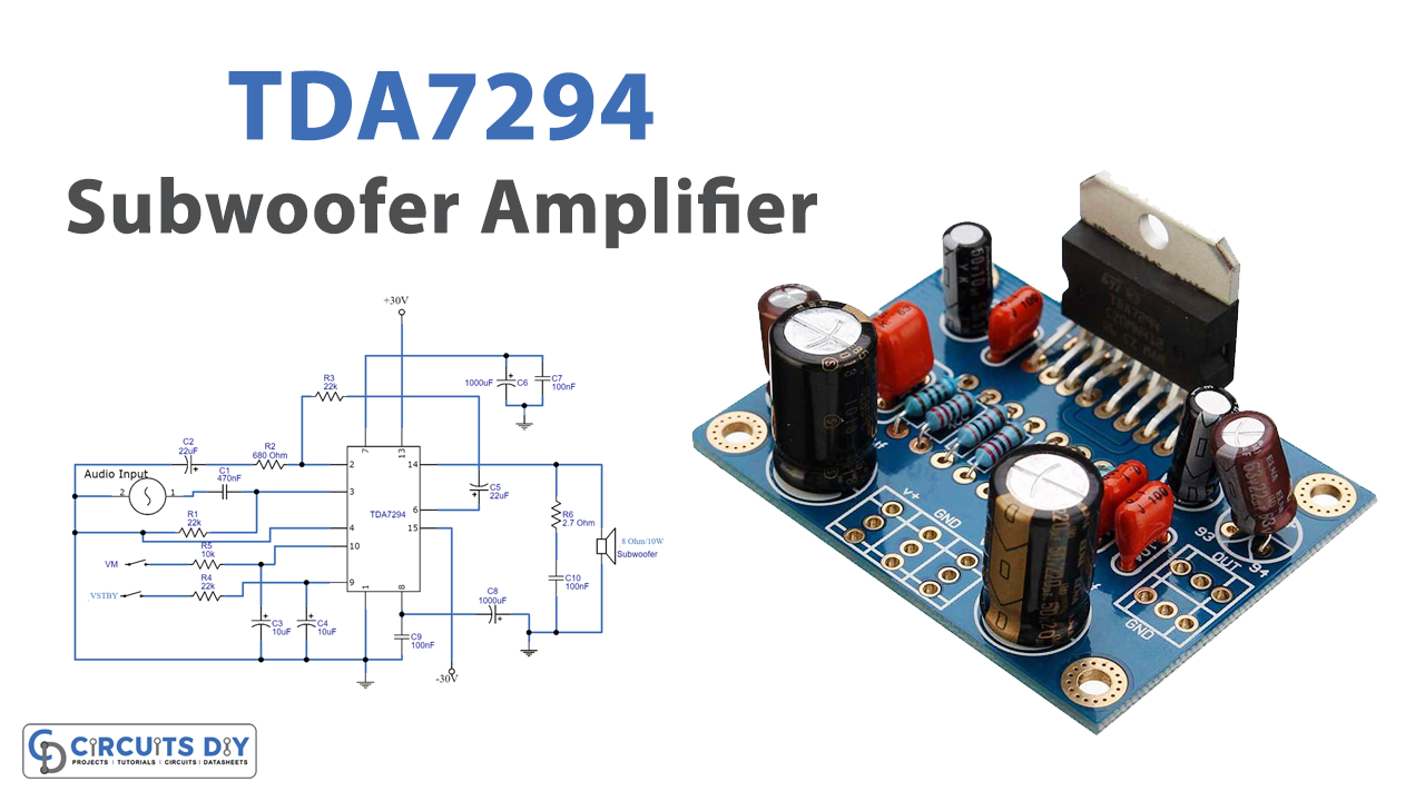
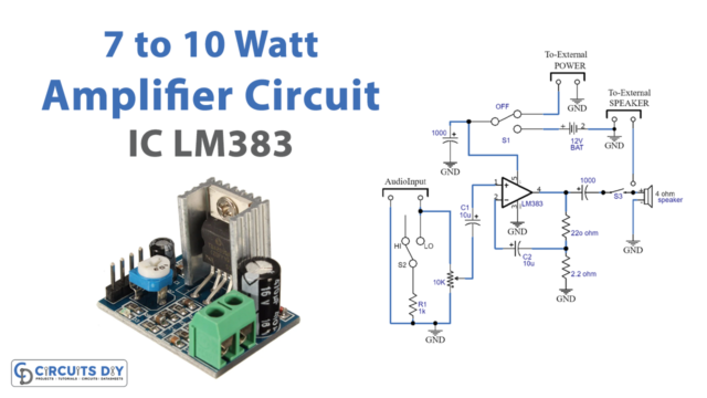
In this tutorial, we are going to make a “TDA7294 Subwoofer Amplifier Circuit”. A subwoofer (or sub) is a loudspeaker designed to reproduce low-pitched(bass and sub-bass) audio frequencies. These frequencies are lower than those which can be generated by a woofer. The typical frequency range for a subwoofer is about 20–200 Hz for consumer products and below 100 Hz for professional live sound. They can never be used alone, as intended to augment the low-frequency range of loudspeakers that cover the higher frequency bands. While the term “subwoofer” technically only refers to the speaker driver.
We need a power amplifier to drive a high-power subwoofer loudspeaker, then only we can get perfect bass sound from the input audio signal. Here we design a subwoofer amplifier circuit by using IC TDA7294 with minimum external components. The IC TDA7294 comes in a multi-watt package, it can be easily connected with a heat sink. This IC has thermal shutdown and short-circuits protection. And due to the wide voltage range and high out current capability, it is able to supply the highest power into both 4Ω and 8Ω loads. Even in presence of poor supply regulation, with high supply voltage rejection. The built-in muting function with turn-on delay simplifies the remote operation avoiding switching on-off noises. This IC can give up to 100 watts of output power, you can use a 30V dual power supply (+30V GND -30V) as a power source.
Hardware Required
| S.no | Component | Value | Qty |
|---|---|---|---|
| 1. | IC | TDA7294 | 1 |
| 2. | Resistor | 22KΩ,10KΩ,680Ω,2.7Ω | 3,1,1,1 |
| 3. | Capacitor | 10uf,22uf,1000uf,100nf | 2,2,2,3 |
| 4. | Speaker | 8Ω/150W | 1 |
| 5. | VM | – | 1 |
| 6. | VSTBY | – | 1 |
| 7. | Connecting Wires | – | – |
| 8. | Dual Power Supply | +30V GND -30V | 1 |
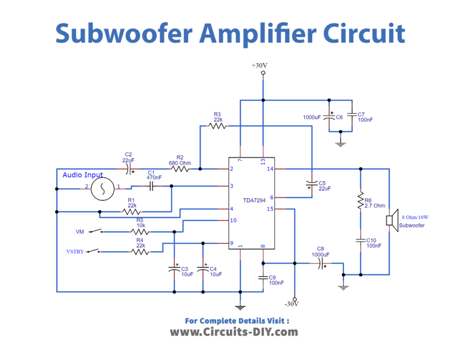
Circuit Diagram
IC TDA 7294
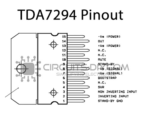
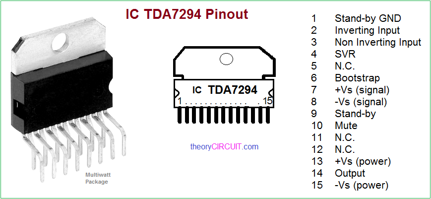
IC TDA7294- 100W DMOS audio amplifier is a monolithic integrated circuit, it comes in multiwatt15V and multiwatt15H packages with a mute option from ST. As IC has mute and stand-by functions to mute the audio output the pin 10 (Vm) should be less than 1.5V and the mute pin 10 (Vm) should be greater than 3.5V. The IC has low noise, low distortion, and good ripple rejection. It can be operated from a wide range of supply voltages. The typical input resistance of TDA7294 IC is 100KΩ and quiescent current is approximately 30mA and its maximum value is 65mA.
Working Explanation
In this circuit, an 8Ω 150W subwoofer speaker is used for a good result. And you can use 50V or above 30V rated capacitors in the amplifier circuit. Here IC TDA7294 is configured to provide 100W output power into an 8Ohm loudspeaker at +/- 30V supply. C1 is the input coupling capacitor and the input is applied to the non-inverting input (Pin3) of the IC. C8 and C6 are power supply filter capacitors while C9 and C7 are bypass capacitors. C5 is the bootstrap capacitor. RC network comprising R1 and C1 improves the high-frequency stability of the amplifier and also prevents oscillations. R5 and C3 set the mute time constant while R4 and C4 set the standby time constant. VM, mute switch, and VSTBY are the standby switch. If you don’t want to use the VM and VSTBY functions leave these pins open & make sure the presence of threshold voltage on these pins. R1 is the input resistance and the amplifier’s input impedance has a direct relationship to its value. R2 and R3 are used for setting type closed loop gain with the used value, the gain is 30dB. C5 is a feedback capacitor, it also provides DC decoupling. Now connect the audio input signal to the non-inverting pin. If you want stand-alone volume control then use a 10KΩ variable resistor at the non-inverting pin followed by audio input. You can easily assemble this circuit on a common prototype board, after completing the circuit construction apply a dual 30V power supply.
Applications
Used in Hi-Fi field applications such as home stereo, self-powered loudspeakers, and top-class TV.


